USJC provides Contract manufactuaring servise of Semiconductor as a member of UMC in Taiwan (the world's third largest foundry).
We have one of the largest 12 inch Logic LSI plant in Japan and produce 38,400 wafers/month.
We implements proactive disaster mitigation measures, including the installation of earthquake-resistant structures, establishment of Li-capacity backup power supply, and deployment of LNG satellite bases.
USJC Strengths
Business Area

-

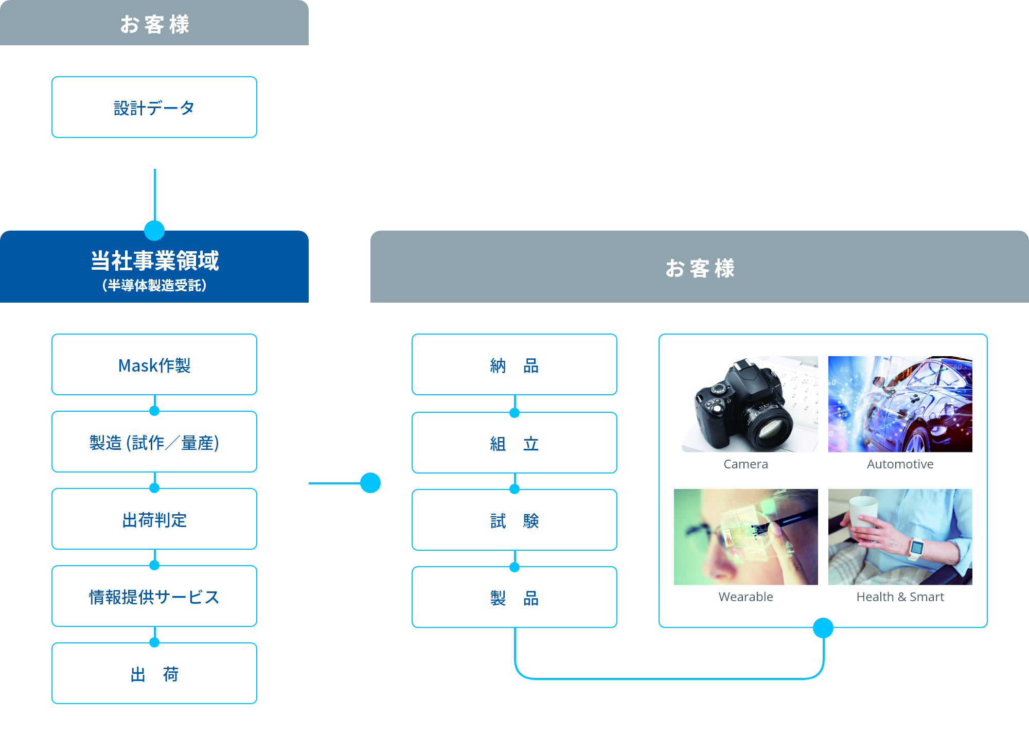
Foundry Service
USJC offers a range of services that cover everything from design support to manufacturing. Our customers benefit from our extensive 40 years of experiences, allowing us to provide speedy and efficient solutions to meet their needs.
Learn More
-
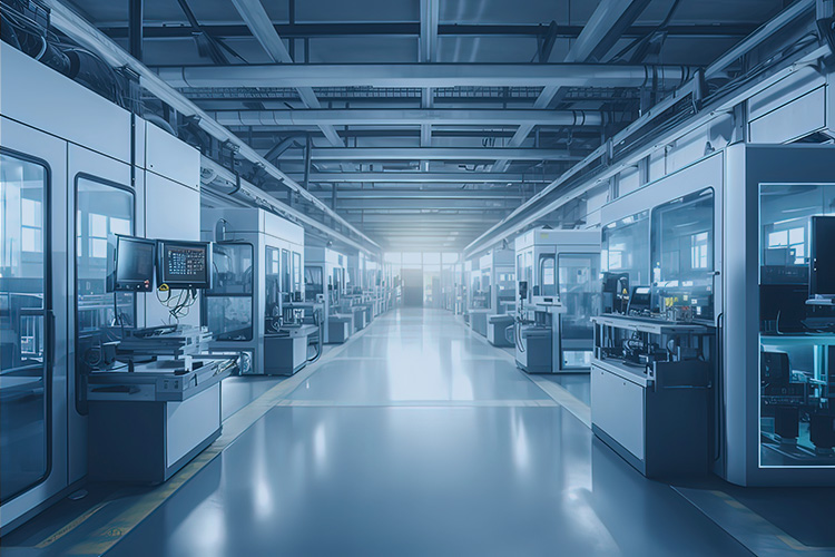
MyUSJC
Our foundry information service, MyUSJC, provides customers with access to our design technology offerings, customer product information, and measurement results.
Learn More
-
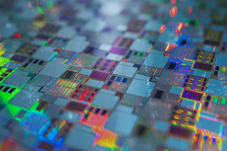
Shuttle Service
The shuttle service is a prototype service using a Multi Project Wafer (MPW). By allowing several customers to share masks and wafers, chip prototyping can be completed at a reduced cost.
Learn More
-
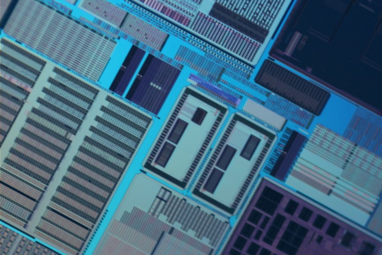
Technology
Together with our customers, USJC aims to contribute towards the realization of a smart society through the technologies and services we provide. Our advanced technology and support allow us to produce products that support the development of a smarter society.
Learn More
-
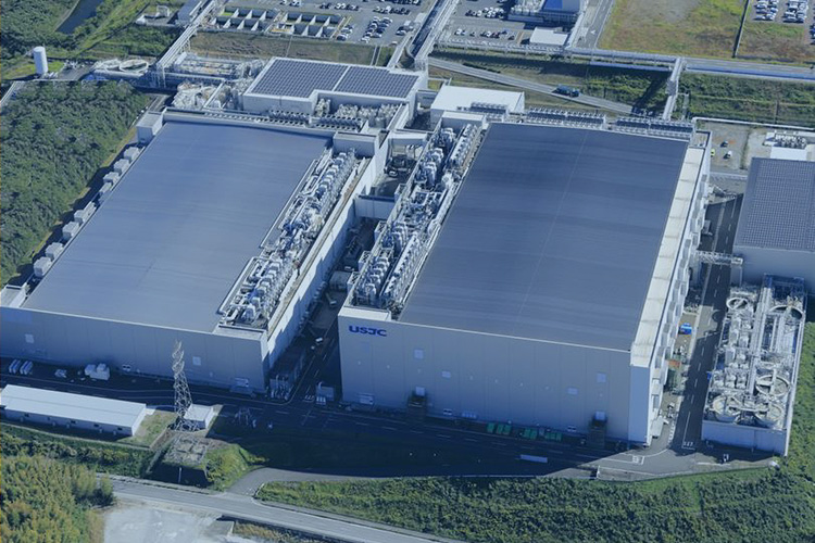
Mie Plant
Surrounded by an abundance of water and rich natural environment, the Mie Plant aims to be an advanced semiconductor manufacturing fab that maintains harmony with the natural environment.
Mie Plant certified to Environment Management System(EMS) "ISO14001"Learn More
-

Domestic Sales
USJC sales team is available to assist customers in Japan with accessing UMC Group's fab capacities and technology.
Learn More
USJC History
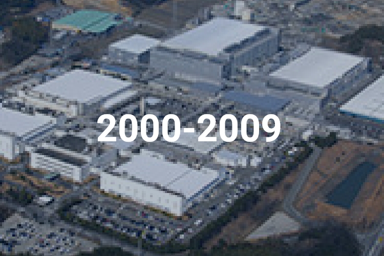
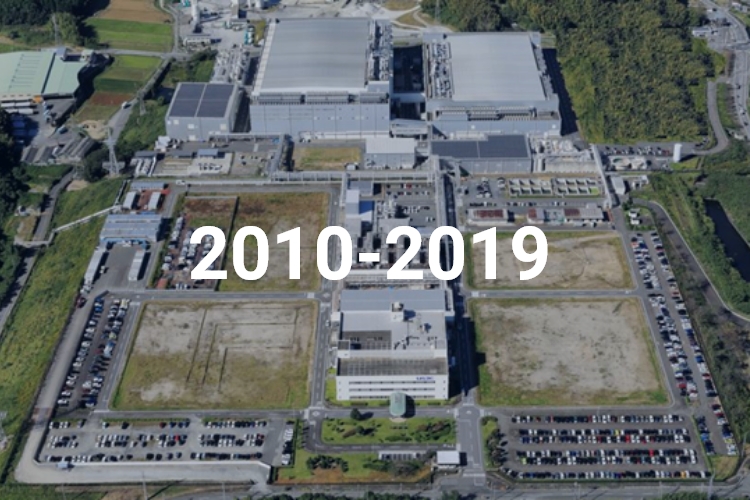
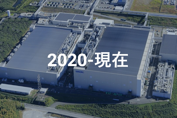
Mie Plant has played a crucial role in the expansion of Japan's semiconductor industry since its establishment in 1984 as a platform for developing prototypes and manufacturing logic, bipolar, and memory products.
Here is a brief overview of its advancement.
History of Mie Plant
~ From the Birth of Semiconductor to the Present ~
1984
Establishement of Mie Plant
In October, Mie plant was established and started operation of Fab-1 (150㎜) for prototypes and mass production of large scale memory and large gate-array
1985
First shipment of EPROM Products
1988
In September, Fab-2 (150㎜) started operation
1991
In July, Fab-3 (200㎜) started operation.
1992
Establishment of the world's first mass production fab for GaAs IC in Japan Development of the world's first CMOS based vector processing LSI (Super computer's operation function is in one chip)
1995
Mie Plant was certified to ISO9001 (1994 Version)
1996
Mie Plant was certified to ISO14001 (1996 Version)
1998
Fab-2 changed to 200㎜ from 150㎜
2003
Started mass production of 90㎚ Cu multilayer wiring
2004
Completion of new 300㎜ wafer manufacturing fab (Fab-B1) at Mie Plant
FPGA's foundry agreement with Lattice Semiconductor (U.S.)
2005
Fab-B1 started production of 90㎚ products in April
In September, initial introduction of NAS battery
2006
Establishment of 2nd 300㎜ manufacturing fab (Fab-B2)
In September, concluded a license agreement with MoSys Inc. to use “IT-SRAM®”, an embedded memory technology, based on 65㎚ process
2007
Fab-B2 started production of 65㎚ products
Success in generating and recovering high purity stone from concentrated hydrofluoric acid wastewater
2008
Spin-off of Fujitsu Limited Semiconductor Business Unit as Fujitsu Microelectronics Limited
In August, ISO/TS16949 was certified
2009
The headquarter of MIFS relocated to Shin-Yokohama Central Building (JR Station Building)
2010
Change of the company name to Fujitsu Semiconductor Limited
Production start of LSI for Supercomputer “K”
2012
Success in breeding "killifish" bred for monitoring water discharge
2013
In April, LNG satellite base was installed in the factory
In September, mass production of DDC transistors based products started
In December, developed manufacturing technology to embed Flash memory cell in logic circuit with DDC technology
2014
In December, Mie Fujitsu Semiconductor Limited was established with capital participation by UMC (Taiwan)
Establishment of Mie Fujitsu Semiconductor Limited
2015
In April, MIFS acquired IPR (intellectual property right) of ultra low power technology from SuVolta
In November, a new clean room adopted SWIT(Swirling Induction Type HVAC system)
2016
In April, MIFS announced partnership with Kilopass in the field of technology development
In April, MIFS made an announcement of combining Deeply Depleted Channel (DDC) and near/sub-threshold technologies to reduce energy
In August, MIFS and FSL announced an agreement with US-based Nantero, Inc. to license that company's technology for NRAM, non-volatile RAM using carbon nanotubes, and to conduct joint development
MIFS was certificated ISO 9001:2015
Mie Plant was certificated IATF 16949:2016
2019
Corporate headquarter and Shin-Yokohama Design center are relocated to Yokohama
MIFS was certified to ISO14001:2015
UMC Receives Final Approval for 100% Acquisition of Mie Fujitsu Semiconductor
Establishment of United Semiconductor Japan Co., Ltd.
2020
In July, USJC was certificated ISO/ICE 27001:2013
2021
In July, USJC was certificated ISO22301:2019
2022
In April, Collaboration with DENSO to production of power semisonductor
USJC was certificated ISO45001:2018
2023
In April, USJC was certificated "ISO27001:2022"
In May, DENSO and USJC started mass production shipment of automotive IGBT
2025
In August, USJC was certificated "IECQ QC 080000:2017"

